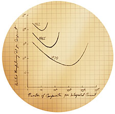
Novedades sobre la ley de Moore en el New York Times de hoy:
"I.B.M. researchers plan to describe an advance in chip-making on Monday that could pave the way for new generations of superchips. The development, which comes from materials research in the design of advanced lenses and related technologies, will make it possible to create semiconductors with wires thinner than 30 nanometers, one-third the width in today's industry-standard chips."
Nota copiada en "comments".
Imagen: el dibujo original de Gordon Moore explicando su predicción.
20.2.06
"I.B.M. Researchers Find a Way to Keep Moore's Law on Pace"
Publicadas por
Andrés Hax
a la/s
2/20/2006
![]()
Suscribirse a:
Comentarios de la entrada (Atom)

1 comentario:
February 20, 2006
I.B.M. Researchers Find a Way to Keep Moore's Law on Pace
By JOHN MARKOFF
SAN FRANCISCO, Feb. 19 — I.B.M. researchers plan to describe an advance in chip-making on Monday that could pave the way for new generations of superchips. The development, which comes from materials research in the design of advanced lenses and related technologies, will make it possible to create semiconductors with wires thinner than 30 nanometers, one-third the width in today's industry-standard chips.
The advance potentially clears one of the biggest hurdles facing the progress of Moore's Law, the observation of Gordon E. Moore, a co-founder of the Intel Corporation, that the density of chips doubles roughly every two years. Mr. Moore made the observation about chip-making technology in 1965, and most semiconductor engineers now believe that the doubling rate will continue through at least the middle of the next decade.
Currently, the densest computer memory chips store 4 billion bits of information; the extension of Moore's Law might make possible a generation storing 64 billion bits by 2013. Such a chip could store roughly 2,000 songs based on today's storage standards.
The industry now uses advanced laser light sources to photo-etch wire lines that are finer than the wavelength of light itself. This is done by generating interference patterns that allow subwavelength resolution. But there had been a general consensus in the industry that this technology would fail below 40 nanometers, requiring a shift to X-ray light sources or other printing technologies.
A group of I.B.M. researchers who collaborated with a team from JSR Micro, an advanced materials company based in Sunnyvale, Calif., will present papers describing the advances at an industry technical conference on photolithography to be held in San Jose, Calif., beginning Monday.
The researchers have created the thinnest line patterns to date using deep ultraviolet lithography, the laser technology used to print circuits on chips. The research has yielded a set of ultrafine lines, each only 29.9 nanometers in width. (A nanometer is a billionth of a meter.)
I.B.M. technologists said the demonstration reduced the risk in the decisions being made by the industry as to which technologies to bet on as many as five years in the future.
"We would like to show a pathway to continue optical lithography," said Robert D. Allen, manager of lithography materials at the I.B.M. Almaden Research Center.
The industry has also been pursuing X-ray light sources as a path to the future. That technology, however, would require that the semiconductor manufacturing industry be drastically revamped. For example, using X-ray light sources would require the industry to use mirrors rather than optical lenses to focus the X-ray sources.
The advance also indicates that the industry has found a way to continue to extend the life of argon fluoride excimer lasers that generate the ultraviolet light used in the photolithographic process. Those lasers have a wavelength of 193 nanometers, yet they are now used commercially to create chips with components as fine as 65 nanometers.
The key to pushing the technology further is a fluid immersion process for conducting the light onto the material that is etched to form the circuit pattern.
The researchers discovered that they could enhance the resolving power of the light source by shifting to a lens made from a crystalline quartz material and exotic immersion liquids that have better refraction properties than those currently used by the industry.
"This is significant," said Fred Zieber, a semiconductor industry analyst at Pathfinder Research. He noted, however, there is more required to turn this into a commercial lithographic process.
The I.B.M. researchers performed their research on a custom piece of equipment they call Nemo, referring to the character in Jules Verne's novel "20,000 Leagues Under the Sea."
http://www.nytimes.com/2006/02/20/technology/20chip.html?_r=2&oref=slogin&pagewanted=print
Publicar un comentario